
Nano Characterisation
The Henry Royce Nanocharacterisation Laboratory at The University of Sheffield is a state-of-the-art facility which contains equipment able to probe the structure, composition, and mechanical properties of all materials at the nanoscale.
The laboratory contains a number of atomic force microscopes, nanoindenters and optical profilers.
These capabilities are open to the UK industrial and academic communities to carry out high-quality nanocharacterisation on novel materials from optoelectronics to RNA therapeutics.
Our equipment:
| Bruker | Contour Elite K |
| Bruker | Dimension XR AFM |
| Bruker | Dimension ICON |
| Bruker | MultiMode 8 |
| Bruker | Resolve |
| Hysitron | TI Premier |
| Micro Materials | NanoTest Vantage |
Bruker Contour Elite K
3D optical microscope with a through transmission media cell and objective to image the corrosion of materials in situ.
Detailed description
The Contour Elite K uses white light interferometry to examine the surface of samples. It has the ability to measure nanometre roughness on large mm2 area.
It can be used to examine a wide range of samples from 0.05% till 100% reflectivity, flat to rough and slopped surfaces, providing accurate measurements plus high-fidelity imaging.
Detailed specifications
- Colour high resolution CCD
- 0.55x zoom lens
- 5x, 20x, and 50x objectives
- TTM module with 20x objective
- Fast measurements 10s to 1min per image (including analysis)
Vision 64 and Vision 64 Map software provides a streamlined user interface that simplifies measurements and analysis.
Location
Royce Discovery Centre, Harry Brearley Building, 5 Portobello Street, Sheffield, S1 4ND
Back to Equipment List
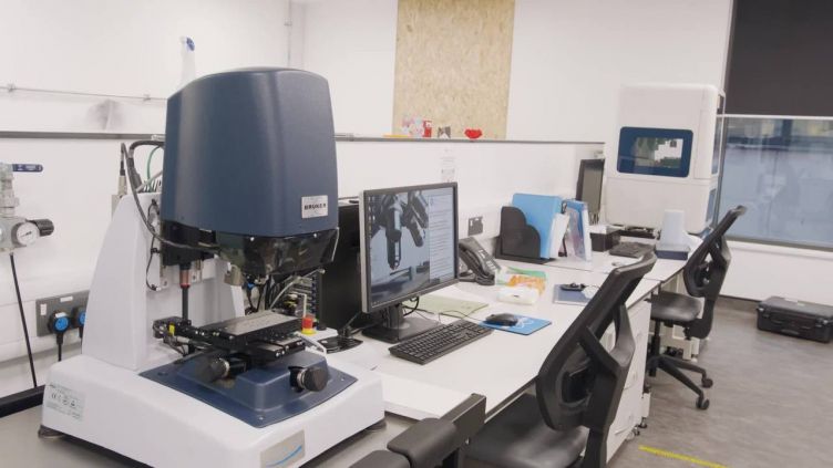
Bruker Dimension XR AFM
The Dimension XR NanoElectrochemical (NanoEC) is part of Bruker's extreme research (XR) series of scanning probe microscopes (SPM). This cutting-edge SPM is configured for the nanoscale electrochemical characterisation of materials in liquids and chemically reactive environments.
Uses/applications
The Dimension XR NanoEC can be used for the electrochemical and electrical characterisation of a wide range of materials and systems including: energy storage systems e.g. lithium-ion batteries, corrosion studies, biosensors, semiconductors, conductive nanotubes and nanoparticles, polymers, and composites.
Detailed description
The Dimension XR NanoEC SPM utilises Bruker's PeakForce Tapping technology and features the AFM-based PeakForce Scanning Electrochemical Microscopy (PF-SECM). PF-SECM performs the simultaneous nanoscale mapping of electrochemical, electrical, and mechanical properties in solution. High resolution topographical images can also be simultaneously acquired.
The electrochemical cell is compatible with a wide range of solutions and liquids including many solvents. The Dimension XR NanoEC has Bruker's DataCube-SECM analysis software which generates 3D data maps where a specific electrical parameter is plotted in XY as a function of one other operating condition. The Dimension XR NanoEC has additional specialised imaging modes which widen its range of application.
The PeakForce TUNA module allows high sensitivity, high resolution current mapping to be performed on fragile samples such as: organic photovoltaics, conductive nanotubes, and nanoparticles. The module has precise force control and eliminates lateral forces preventing sample damage. The current range covered is from pA up to nA.
The PeakForce Kelvin Probe Force Microscopy (PF-KPFM) module performs nanoscale surface potential mapping with both frequency modulation and amplitude modulation. The Scanning Capacitance Microscopy module maps the change is electrostatic capacitance between the scanned probe and the surface of a sample. This imaging mode can be used to map the relative changes in carrier concentrations in semiconductors.
The accompanying Dark-Lift software enhances the mapping accuracy and eliminates photoelectric artefacts. The Dimension XR NanoEC has an additional FastScan option which is capable of producing high quality images at scan rates of 20Hz compared to standard imaging rates of 1Hz.
Detailed specifications
Imaging modules: PeakForce SECM with DataCube - SECM analysis software, PeakForce TUNA with DCube - TUNA, PeakForce KPFM, PeakForce SCM with DarK-Lift software, FastScan.
Scanner: Icon Scan Head - Maximum scan area 90μm x 90μm with 10μm Z range; FastScan Scan Head - Maximum scan area 35μm x 35μm with 3μm Z range.
Sample size: 210mm diameter and 15mm thickness maximum.
Location
Royce Discovery Centre, Harry Brearley Building, 5 Portobello Street, Sheffield, S1 4ND
Back to Equipment List
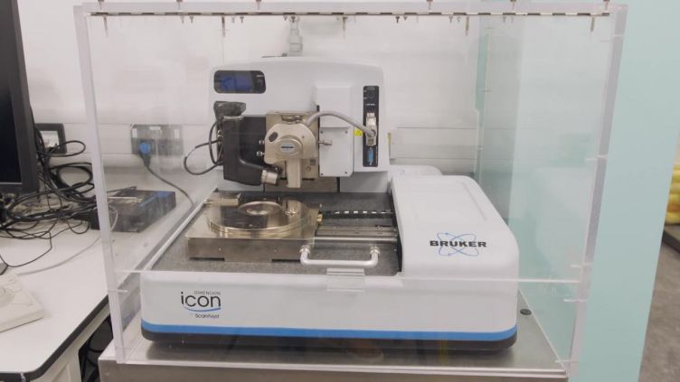
Bruker Dimension ICON
The Bruker Dimension ICON large-sample AFM is an easy to use, high resolution instrument capable of AFM modes including contact, tapping, and peak-force quantitative nanomechanical mapping.
Uses/applications
The Dimension ICON is used wherever the nano/micro scale topography and mechanical properties are imperative to the functioning of the device. This can be the analysis of tough surface coatings all the way to hydrogels.
Detailed description
AFM allows surface topology to be mapped down to the nanometer scale. The Icon is a culmination of Bruker's industry-leading, ti-scanning AFM technology, incorporating temperature-compensating position sensors to render noise levels in the sub-angstrom range for the Z-axis, and angstroms in XY.
This is extraordinary performance in a large-sample, 90-micron scan range system, surpassing the open-limo noise levels of high-resolution AFMs. The new design of the XYZ closed-loop head also delivers higher scan speed, without loss of image quality, to enable greater throughput for data collection.
Bruker-exclusive PeakForce Tapping® enables the Dimension Icon to routinely create the highest resolution images. Utilises PeakForce Tapping® technology, PeakForce QNM® maps, and distinguishes between nano mechanical properties - including modulus, adhesion, dissipation, and deformation.
Location
Royce Discovery Centre, Harry Brearley Building, 5 Portobello Street, Sheffield, S1 4ND
Back to Equipment List
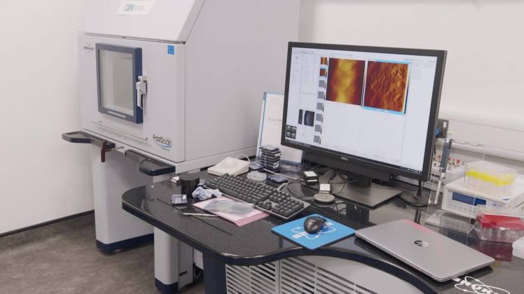
Bruker MultiMode 8
The MultiMode 8 is a multifunctional high resolution atomic force microscope.
Uses/applications
Due to its versatility, the MultiMode 8 can be used to study and characterise a wide range of materials, including: Biological material, Polymers, 2D materials, Metals, Composites, and Ceramics.
Detailed description
The MultiMode 8 has Bruker's PeakForce Tapping technology in addition to the standard AFM imaging modes. This technology gives high resolution AFM imaging of a wide range of materials from soft biological samples to hard materials in both air and liquid. Included in this technology is PeakForce QNM which allows for the quantitative nanoscale mapping of nano mechanical properties including modulus, adhesion, and deformation, whilst simultaneously imaging sample topography.
Additionally, the MultiMode 8 has a PeakForce-HR module which facilitates PeakForce Tapping at scan speeds 6x faster than traditional imaging modes without any loss in image quality. For novice users, the MultiMode 8 has ScanAsyst for automatic image optimisation which eliminates the need to manually adjust complicated imaging parameters.
Detailed specifications
System: NanoScope V controller and NanoScope 9.2 software
Scanner: Maximum 170μm x 170μm scan area with 6μm Z range
Imaging modules: PeakForce Tapping, PeakForce QNM, PeakForce-HR ScanAsyst
Specimen size: 12mm x 12mm x 5mm maximum
- Standard modes including tapping, contact, phase, and magnetic
- Fluid Cell for imaging in liquids
Location
Royce Discovery Centre, Harry Brearley Building, 5 Portobello Street, Sheffield, S1 4ND
Back to Equipment List
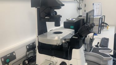
Bruker Resolve
The Bruker Bioscope Resolve is a Bio-AFM combined with an inverted Nikon TI2 fluorescence microscope, allowing correlated simultaneous high resolution imaging and topography. The instrument is capable of nano mechanical mapping, and complex indenter ramps, making coordinated fluorescent images with nano-scale force information in near physiological conditions.
Uses/applications
- High resolution imaging of biological samples in buffer solution (tissues, cells, viral particles, hydrogels applications, biomedical devices, and individual biomolecules)
- Studies of nano-scale forces between ligands in the single molecule range (Molecular interaction mapping, Single Molecule Force Spectroscopy (SMFS))
- Correlated fluorescence and atomic force microscopy (AFM) operation for high-resolution data collection and functional targeting of samples of interest (e.g. tissues, surfaces, and cells).
Detailed description
- High-resolution multimodal AFM imaging for all scan ranges from cells and tissues to single molecules
- Lateral AFM scan range up to 100μm, vertical range (height) up to 15μm. Vertical resolution typical <0.5 nm
- Comprehensive Package for live cell and tissue imaging and nano-mechanical mapping
- Small volume capabilities (~60μl) with sample perfusion for molecular biology and single molecule applications
- Fast scanning options for live cell imaging and single molecular scanning (up to 98Hz) in liquid
- Software controlled heating stage from ambient temperatures to ~60ºC
- Semi-automated fluorescence image acquisition and device control and a wide range of image analysis options and correlation with AFM images
- Wide range of suitable for sample and substrates: Glass coverslips up to 75x25mm, plastic and glass bottom Petri dishes from 35-60mm
- Easy sample access and navigation by a long range fulling motorised X-Y-Z stage
- A top view camera for optical brightfield observation of opaque samples.
Detailed specifications
- High resolution imaging of biological samples in buffer solution (tissues, cells, viral particles, hydrogels applications, biomedical devices, and individual biomolecules)
- Studies of nano-scale forces between ligands in the single molecule range (Molecular interaction mapping, Single Molecule Force Spectroscopy (SMFS))
- Correlated fluorescence and atomic force microscopy (AFM) operation for high-resolution data collection and functional targeting of samples of interest (e.g. tissues, surfaces, and cells)
Location
Royce Discovery Centre, Harry Brearley Building, 5 Portobello Street, Sheffield, S1 4ND
Back to Equipment List
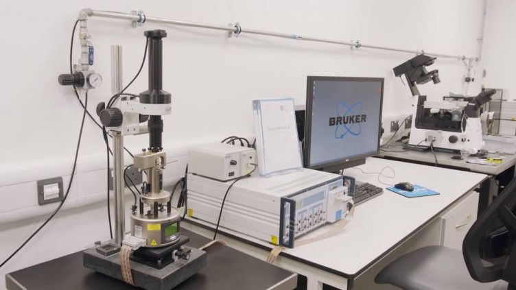
Hysitron TI Premier
The Hysitron TI Premier triboindenter is a nanoindenter used primarily to calculate the hardness and reduced modulus of a material. The indentation depth vs force plots can be used to determine surface coating thickness.
Uses/applications
The TI Premier is commonly used to determine mechanical properties from everything from biological samples to diamond coatings. It's commonly used to characterise alloys for quality control and development.
Detailed description
Features:
- 20 X microscope allows for precise indentation location (+/- 20nm)
- 10mN maximum force, 1 nN resolution
- 0.04 nm displacement resolution
- Berkovich diamond indenter
- Vertical indentation direction
- Indentation automation
Location
Royce Discovery Centre, Harry Brearley Building, 5 Portobello Street, Sheffield, S1 4ND
Back to Equipment List
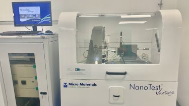
Micro Materials NanoTest Vantage
The NanoTest Vantage combines multiple nano mechanical and nanotribological test techniques over multiple force scales and temperatures.
Uses/applications
The NanoTest Vantage can be used to study a wide range of materials systems for both research and industrial applications including: Metals, Polymers, Ceramics, Glass, Composite materials, Hard coatings, and Thin films.
Detailed description
The NanoTest Vantage has a high degree of functionality and can be used to study a wide range of materials for both research and industrial applications. The test techniques available include indentation, scratch, wear, friction, and impact. Two load modules are available, a low load module with a load range of 10μN to 500mN and a high load module with a range of 300mN to 30N. The NanoTest Vantage is ideally suited for testing materials at elevated temperatures up to 500°C due to its unique design.
The stage configuration allows large samples to be accommodated with a maximum testable sample area of 100mm x 50mm and a maximum sample thickness of 150mm. The post experiment analysis software has a wide range of capabilities including creating hardness and modulus maps in both 2D and 3D and producing stress-strain curves from experimental data.
Detailed specifications
- The NanoTest Vantage has a NanoTest NTX4 system controller and a high accuracy National Instruments data acquisition system with NI-MCal calibration technology.
- Platform 4 software allows for instrument control, experiment design, and data analysis.
- Up to 100 experiments can be defined and queued to run automatically.
- Maximum sample size: 100mm x 50mm x 150mm.
- Temperature range: Up to 500°C.
- Indentation: Load range available 10uN to 500mN with low load head, 300mN to 30N with high low head.
- Scratch module: Maximum friction force 250mN, Maximum scratch distance 10mm, Scratch speed 100nm/s to 0.1mm.
- Impact module: Acceleration distance up to 20μm, Strain rate at contact up to 104s-1.
Location
Royce Discovery Centre, Harry Brearley Building, 5 Portobello Street, Sheffield, S1 4ND
Back to Equipment List
Enquire: royce@sheffield.ac.uk