Electron optics
Information on equipment available for electron optics.
Off
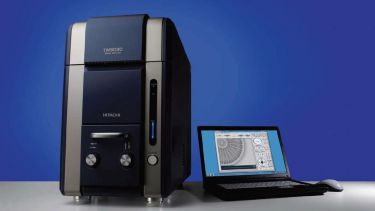
Scanning Electron Microscopy with Energy Dispersive Spectrometry, Hitachi TM3030 (M06)
Routine imaging and spatially resolved elemental analysis of solid and powder materials.
- Low vacuum mode for investigation of non-conducting samples (ESEM)
- Magnification 30x to 30,000x
- Accelerating voltage of 5-15 kV
- Sample size up to 70 mm in diameter and 50 mm thickness
- Oxford Instruments Quantax 70 EDX detector for microanalysis and element mapping
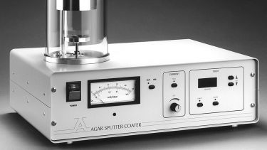
Carbon coater, Agar Scientific (M06)
Routine coating of SEM and microprobe samples.
- Dual carbon rod source with current feedback for reproducible carbon coating
- Manual and pulse mode for heart sensitive samples
- Film thickness monitor for accurate control of coating thickness if required
- Standard sample holder holds 12 x 12.5 mm diameter Agar specimen stubs
- Height of sample stand is adjustable to give a working distance between 25 and 65mm
Ion beam polishing (Sorby Centre)
Preparation of extremely high quality SEM and TEM specimens using ion beam polishing.
- Gatan Ilion II system
- For preparation of damage free cross sectional SEM specimens
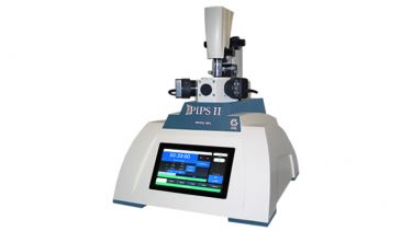
- Gatan PIPS II system
- For preparation of high quality TEM specimens with exceptionally large, clean and transparent areas
- Programmable user protocols for high reproducibility
Advanced electron optics (Sorby Centre)
Access to state of the art facility for high resolution imaging and chemical analysis of materials.
- Tecnai 20 TEM with CCD and EDX system for high resolution imaging
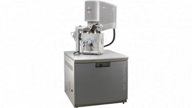
- FEI Sirion FEG-SEM with EBSD for ultra-high resolution imaging
- FIB SEM for TEM sample preparation
- Several high resolution TEM and SEM systems with EDX capability
- Note – analysis of radioactive materials is possible only with selected equipment


