
Research activities
Our research covers many III-nitrides topics and leading achievements in areas ranging from novel epitaxial growth to device fabrication.
Our research on III-nitride semiconductor devices includes nanophotonics, electronics, hybrid III-nitride/polymer optoelectronics, integration of photonics and electronics, flexible devices, micro-LEDs and solar energy devices.

You can see these research interests in greater detail below:
- MOVPE Growth Capacities
-
Development of advanced overgrowth techniques to allow the growth of high-quality GaN on substrates in non-polar and semi-polar orientations.
- GaN on sapphire: 4 and 2 inch (Polar; non-polar; semi-polar )
- GaN on Silicon: (111), (110), (311), (411)
- GaN on SiC: 6H
- GaN on Diamond: (111) and others
- Advanced Manufacturing Capabilities

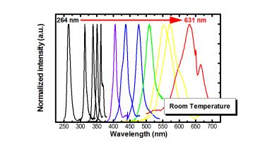
MOVPE epitaxial growth of III-nitrides (AlGaN, GaN, InGaN) from deep UV to the whole visible spectral region - Monolithic integration of LED-HEMT
-
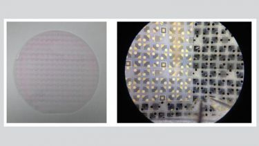
- Demonstration of Epitaxial Integration of LEDs-HEMTs on up-scalable substrates
- Epitaxial integration of µLED & RF on semi-/non-polar GaN on up-scalable Substrates
- Individually addressable µLEDs/RF with multiple colours
- Ultra-fast visible light wireless communication
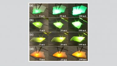
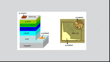
Controllable Uniform Green Light Emitters Enabled by Circular HEMT-LED Devices
Yuefei Cai, Yipin Gong, Jie Bai, Xiang Yu, Chenqi Zhu, Volkan Esendag, Kean Boon Lee, Tao Wang
IEEE Photonics Journal (2018), doi: 10.1109/JPHOT.2018.2867821 - III-nitride Micro-LEDs for micro-display and Li-Fi
-
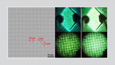
- Epitaxial growth of µLEDs/HEMTs on sapphire
- IQE increases with decreasing dimension, which is opposite to all the µLEDs reported so far.
- Major advantage: eliminating any etching induced damages
- Three patents on μ-LEDs have been filed
A Direct Epitaxial Approach To Achieving Ultrasmall and Ultrabright InGaN Micro Light-Emitting Diodes (μLEDs)
J. Bai, Y. Cai P. Feng, P. Fletcher, X. Zhao, C. Zhu & T.Wang
ACS Photonics (2020), doi: 10.1021/acsphotonics.9b01351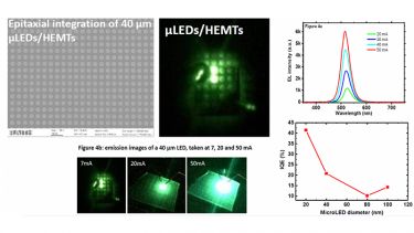
- Long wavelength semi-polar III-nitride emitters
-
- Greatly enhanced crystalline quality of our 5µm GaN (XRD FWHM <360”)
- Latest data: XRD linewidth of ~ 0.07 degree at 90 azimuth angle
Topical Review: Development of overgrown semi-polar GaN for high efficiency green/yellow emission
T Wang
Semicond. Sci. Technol. 31, 093003 (2016)
This review presents recent progress on developing semi-polar GaN overgrowth technologies on sapphire or Si substrates, the two kinds of major substrates which are cost-effective and thus industry-compatible, and also demonstrates the latest achievements on electrically injected InGaN emitters with long emission wavelengths up to and including amber on overgrown semi-polar GaN.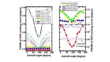

Semi-polar LEDs (Green to Amber)
- Semipolar InGaN LEDs bridge the “green/yellow” gap for ultrafast visible light communications and Opto-genetic applications
- Highlighted by a number of media, “Semiconductor Today”, ”LED Inside”, ”END Asia”
(11-22) semipolar InGaN emitters from green to amber on overgrown GaN on micro-rod templates
J. Bai, B. Xu, F. G. Guzman, K. Xing, Y. Gong, Y. Hou and T. Wang
Appl. Phys. Lett. 107, 261103 (2015)
http://dx.doi.org/10.1063/1.4939132 - Semi-polar GaN on silicon
-
Our approach to patterning (311) Si
Buffered HF to remove the SiO2 layer
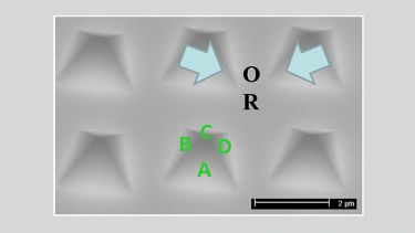
With respect to the surface:
Facets Angle A (111) 29.5° B (1-11) & D(-1-11) 58.5° C (-111) 80.1° - The angle between (11-22) GaN and c-plane GaN is 58.4o
- GaN (c-plane GaN) is grown on B or D facet, leading to the formation of (11-22) GaN along the vertical direction.
- Ideally, GaN is grown only on either B facet or D facet, but not on both
Cross-sectional SEM image
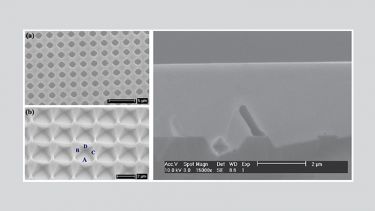
Novel mask-patterned (113) silicon: high quality (11-22) semi-polar GaN on silicon. A further generic approach to achieve different semi-/non- polar GaN Growth and characterization of semi-polar (11-22) GaN on patterned (113) Si substrates
J Bai, X Yu, Y Gong, Y N Hou, Y Zhang and T Wang
Semiconductor Science and Technology, Volume 30, Number 6, 2015 - Electronic devices
-
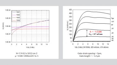
Semi-insulating GaN for electronics
Semi-insulating GaN for power electronics & RF devices for 5G application
- Nano-array blue LEDs
-
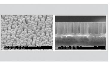
Nanorod array: ~200 nm in diameter and ~1×10 9 /cm2 in density. Good uniformity in 2 inch wafer. 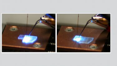
Nano-array blue LED with ultra high efficiency for next generation solid state lighting Publications
Characterization of InGaN-based nanorod light emitting diodes with different indium composition
J. Bai, Q. Wang and T. Wang
J. Appl. Phys. 111, 113103 (2012); http://dx.doi.org/10.1063/1.4725417Influence of strain relaxation on the optical properties of InGaN/GaN multiple quantum well nanorods
Q Wang, J Bai, Y P Gong and T Wang
Journal of Physics D: Applied Physics, Volume 44, Number 39 (2011)Reduced longitudinal optical phonon-exciton interaction in InGaN/GaN nanorod structures
P. Renwick, H. Tang, J. Bai and T. Wang
Appl. Phys. Lett. 100, 182105 (2012); http://dx.doi.org/10.1063/1.4711210Probing light emission from quantum wells within a single nanorod
Jochen Bruckbauer, Paul R Edwards, Jie Bai, Tao Wang and Robert W Martin
Nanotechnology, Volume 24, Number 36 (2013) - Hybrid III-nitride/organic device for white LED
-
The combination of III-nitride based inorganic materials with organic semiconductors allows the development of increased efficiency white light emitting structures. This combines the strengths of both materials classes.
Through the combination with novel nanostructures, it has been possible to utilise high efficiency non-radiative energy transfer coupling between the III-nitride materials and organics.

Hybrid III-Nitride/Organic Semiconductor Nanostructure with High Efficiency Nonradiative Energy Transfer for White Light Emitters
R. Smith, B. Liu, J. Bai, and T. Wang
Nano Lett., 2013, 13 (7), pp 3042–3047
DOI: 10.1021/nl400597d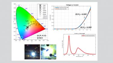
Electrically injected hybrid III-Nitride/organic white LED - Hydrogen generation using GaN nanostructures
-
Solar-powered hydrogen generation
III-nitride photoelectrodes with Nanostructure: high solar-to-Hydrogen efficiency, highlighted in “SPIE” in September/October 2014
This video shows hydrogen gas formation at the counter electrode with oxygen formation at the InGaN semiconductor device under solar illumination:
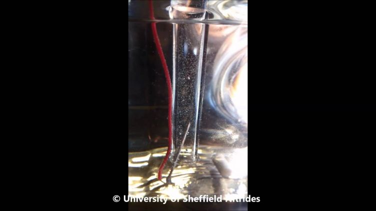
The chemical stability of nitride materials and the widely tuneable bandgap allow efficient conversion of solar energy to hydrogen as a fuel source.
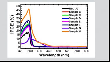
IPCE as a function of wavelength for all the GaN based nanoporous structures and the as-grown structure as reference. © 2014 AIP Publishing LLC Utilisation of GaN and InGaN/GaN with nanoporous structures for water splitting
J. Benton, J. Bai and T. Wang
Appl. Phys. Lett. 105, 223902 (2014)Significantly enhanced performance of an InGaN/GaN nanostructure based photo-electrode for solar power hydrogen generation
J Benton, J Bai and T Wang
Appl. Phys. Lett. 103, 133904 (2013)Enhancement in Hydrogen Generation Efficiency Using A GaN-based Nanorod Structure
J Benton, J Bai and T Wang
Appl. Phys. Lett. 120, 173905 (2013) - UV-LEDs
-
- Non-Line-of-sight (NLOS) communications
- water purification
- Environmental Protection
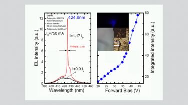
Novel approach for 340 nm UV LEDs
Greatly improved performance of 340nm light emitting diodes using a very thin GaN interlayer on a high temperature AlN buffer layer
T. Wang, K. B. Lee, J. Bai, P. J. Parbrook, R. J. Airey, Q. Wang, G. Hill, F. Ranalli and A. G. Cullis
Appl. Phys. Lett. 89, 081126 (2006); http://dx.doi.org/10.1063/1.2338784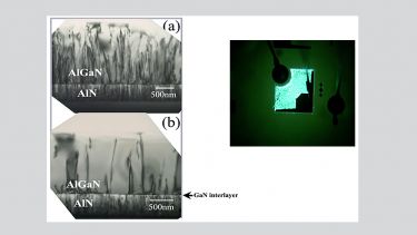
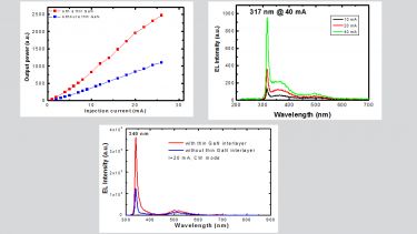
310-340 nm UV LEDs
The 310–340 nm ultraviolet light emitting diodes grown using a thin GaN interlayer on a high temperature AlN buffer
T Wang, K B Lee, J Bai, P J Parbrook, F Ranalli, Q Wang, R J Airey, A G Cullis, H X Zhang, D Massoubre
Journal of Physics D: Applied Physics, Volume 41, Number 9 (2008)
Deep UV emission
Mechanisms of dislocation reduction in an Al0.98Ga0.02N layer grown using a porous AlN buffer
J. Bai, T. Wang, P. J. Parbrook and A. G. Cullis
Appl. Phys. Lett. 89, 131925 (2006); http://dx.doi.org/10.1063/1.2358123
- GaN nanostructures based solar cells
-
Incorporation of nanoscale structures into III-nitride based optoelectronic devices by application of novel, cost-effective device fabrication processes. Allows control over light and carrier dynamics in iii-nitride optoelectronic devices, such as microdisk lasers.
III-nitrides solar Cells
Efficiency enhancement of InGaN/GaN solar cells with nanostructures
J. Bai, C. C. Yang, M. Athanasiou and T. Wang
Appl. Phys. Lett. 104, 051129 (2014)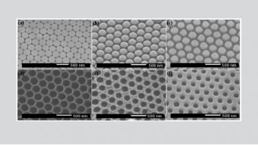
- III-nitride micro-/nano- lasers
-
Room temperature CW plasmonic nano laser with ultra-low threshold
Through the combination of nanoscale metals and III-nitride materials, light-matter interaction can be manipulated. This allows optical fields to be concentrated into sub-diffraction limited volumes.
A plasmonic laser has recently been demonstrated using a single InGaN/GaN nanorod coupled to silver films.
Room temperature plasmonic lasing in a continuous wave operation mode from an InGaN/GaN single nanorod with a low threshold
Y. Hou, P. Renwick, B. Liu, J. Bai & T. Wang
Scientific Reports 4, Article number: 5014 (2014) doi:10.1038/srep05014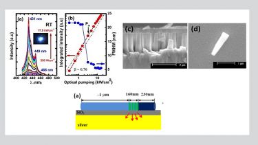
Room temperature optically pumped CW green laser on Si with record-low threshold
Room temperature continuous–wave green lasing from an InGaN microdisk on silicon
M. Athanasiou, R. Smith, B. Liu & T. Wang
Scientific Reports 4, Article number: 7250 (2014), doi:10.1038/srep07250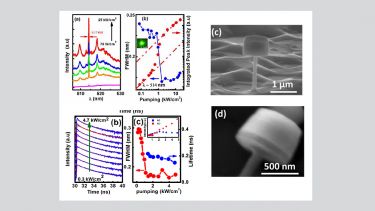
- III-nitrides lasers
-
Blue laser diode - among the few earliest university groups to achieve this world-wide
Demonstration of electrically injected InGaN/GaN based violet/blue laser in collaboration with an overseas team for device fabrication in 2004, achieved then among only a few university groups.
Highlighted in “Nitride Europe”, III-Vs Review 17, 36 (2004)
Publications
Growth and optical investigation of self-assembled InGaN quantum dots on a GaN surface using a high temperature AlN buffer
Q. Wang, T. Wang, J. Bai, A. G. Cullis, P. J. Parbrook and F. Ranalli
J. Appl. Phys. 103, 123522 (2008); http://dx.doi.org/10.1063/1.2939568
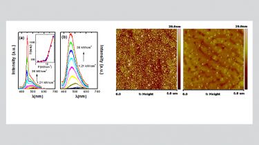
Ultra high density of QDs with high crystal quality: room temperature stimulated emission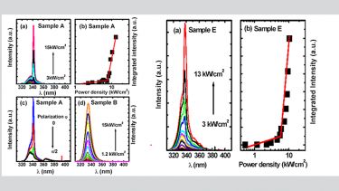
Stimulated emission at 340 nm from AlGaN multiple quantum well grown using high temperature AlN buffer technologies on sapphire
Q. Wang, Y. P. Gong, J. F. Zhang, J. Bai, F. Ranalli1 and T. Wang
Appl. Phys. Lett. 95, 161904 (2009); http://dx.doi.org/10.1063/1.3253416
High temperature AlN buffer technique: RT stimulated emission at 340 nm with a low threshold
Highlighted in “Semiconductor Today” on 28th October 2009Shortest wavelength VCSEL
High quality III-nitride DBR: Shortest wavelength VCSEL at room temperature so far. (Highlighted by “Applied Physics Letters” cover image, shown below)
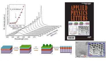
Optically pumped ultraviolet lasing from nitride nanopillars at room temperature
Rui Chen, H. D. Sun, T. Wang, K. N. Hui and H. W. Choi
Appl. Phys. Lett. 96, 241101 (2010); http://dx.doi.org/10.1063/1.3449576 - GaN-based ISB Devices
-
Unique advantages of GaN-based ISB:
- Large conduction band offset =>1.75eV for GaN/AlN, pushing this family of devices to much shorter wavelengths
- 1.3-1.55μm wavelength range used for fiber-optics telecommunications requiring a band offset of ~1 eV
- Ultra short ISB relaxation time (140-400 fs at RT) 10 times faster than in InGaAs QWs, offering the prospect of ultrafast ISB devices. Appl. Phys. Lett. 77, 648(2000); Semicond. Sci. Technol. 19, S463(2004)
- Large longitudinal phonon energy (92meV for GaN compared to 36meV for GaAs) => enable sources emitting in the Reststrahlen band of GaAs and InP and high-performance lasers at THz frequencies


