
Cleanroom
(Room 1.06 - First Floor)

Overview:
The Cleanroom is a specialist environment for the engineers of tomorrow. It has its own air conditioning plant, which allows temperature, humidity and air cleanliness to be tightly controlled. Users must wear special protective clothing and observe stringent operating protocols. The facility is over one hundred times cleaner than a normal laboratory, allowing the definition of features as small as one micron (0.001mm).

The Cleanroom allows students to get real experience of the micron-scale devices that underpin much of modern life, including:
- Microelectronics (resistors; capacitors; diodes; transistors)
- Optoelectronics: Light emitting diodes (LEDs); solar cells; waveguides
- Radio frequency (surface acoustic wave filters; antennae)
- Microsensors (chemical; biochemical; microfluidic)
- Micromechanics (cantilevers; oscillators)

Device manufacture falls into three main process areas: wet chemistry; photolithography and vacuum processing.
The wet chemical processes take place in seven laminar flow cabinets, which enable noxious fumes to be removed.
The photochemical processes are conducted in the Yellow Room, where the air is even cleaner (one thousand times cleaner than outside) and the lights are filtered to remove the blue end of the visible spectrum.
The vacuum processes take place in chambers that can be evacuated to a pressure of 10-9 atmospheres.
By carefully following a predefined sequence of wet chemistry; photolithography and vacuum processing, it is possible to manufacture a near-infinite range of devices.

- Students will learn:
-
- How to work safely and efficiently in the specialist environment of the cleanroom.
- How to design micron-scale devices using industry-standard software.
- How to manufacture micron-scale devices using standard fabrication tools.
- How to perform electrical and optical tests on micron-scale devices.
- What equipment is in this lab?
-
- Plasma etching (oxygen and argon)
- Thermal evaporators
- Inert atmosphere tube furnace
- Desktop rapid thermal annealer (RTA)
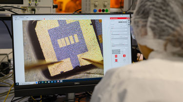
- Optical microscopes with digital cameras
- Probe stations
- Source-measurement units (Keysight B2900)
- LCR meters (Keysight)
- Solar simulator (Newport multi-LED 0-1 sun)
- Spinner
- Mask aligners (LED and mercury arc technology)
- Mask writer (Heidelberg µPG101) Min. feature size = 1µm
- Diamond stylus surface profilometer (Dektak)
- Wire bonder
- Sputter coater (DC and RF)
- Links to Schools and other Departments:
- Which staff are in this lab?
- Request Use of Equipment:
-
Please email mee-cleanroom@sheffield.ac.uk with:
- Your name
- Your degree & year of study
- What equipment you want to use and why
Please allow 3-5 working days for a response.


Visit us
Discover what sets Sheffield apart at our undergraduate open day on Saturday 5 July 2025.