

Electron probe micro-analysis (EPMA) provides a significantly enhanced means to obtain precise and accurate quantitative elemental compositional analysis of complex materials systems at the micron scale. EPMA complements the visual inspection of the microstructure performed in Scanning Electron Microscopy by providing quantitative information about the chemical elements present under the electron beam. It answers key questions for many applications in materials science:
- What elements are present in microstructural features?
- How are they spatially distributed?
- What are their concentrations?
The JEOL JXA 8530F at the University of Sheffield is funded by the Henry Royce Institute. It is equipped with four crystal spectrometers enabling a spectral resolution that surpasses that which can be achieved using conventional energy dispersive spectroscopy (EDS) analysis with sensitivity down to ppm levels. The technique lends itself to a broad range of applications determining the elemental distribution in materials from advanced alloys, nuclear waste forms, ceramics, electrode materials to archeological glasses.
The JXA 8530F Plus is also equipped with a soft X-ray emission spectrometer (SXES) enabling ultra-high spectral resolution, offering the potential for chemical state mapping particularly of light elements. This is particularly of interest when exploring the influence of light elements such as boron in (specific type required) alloys and lithium or sodium in novel battery materials.
The SXES spectrometer uses X-ray focusing optics, variable line-spacing gratings (JS50N and JS200N) and a solid-state X-ray CCD detector to collect a low energy X-ray spectrum. It provides higher spectral resolution and higher sensitivity for soft X-rays (50eV to 210eV) relative to traditional WDS, yielding information on electronic structure and materials bonding from examining the peak shapes. The grating and CCD detector are rigidly fixed, with no moving parts, resulting in spectra that are extremely reproducible. This allows for the analysis of ultra-light elements with very high peak to background ratios.

The JEOL EPMA is utilised by a range of research groups including Advanced Structural Materials, Functional Materials and Devices, Cement and Glass analysis. It is also available for other Departments, other institutions and industrial based projects that require micro analysis.
The Jeol JXA 8350X F plus instrument has been used to provide quantitative micro analysis on a variety of challenging samples.
Our EPMA analytical capabilities, combined with data processing software, form a very powerful and cost-effective tool for academic and industrial research. We offer bespoke analytical set-ups for almost any element (B to U) combination in solids such as minerals, glasses, metals and alloys, and ceramics. Over the last 12 months our EPMA has developed specialist applications for specific researchers and research communities. Instrument calibration is carried out by analysing reference materials with known compositions. A major part of the analysis is to determine for each element of interest, which x-ray line with their order of reflection to use. This is to minimise the effects of peak interference and overlaps on analysis. This together with accurate evaluation of peak scans (profiles) and determination of background positions provide accurate and reproducible results. Routine detection limits are typically 60 – 600 ppm, depending on the element and host material.
Electron microscopy techniques such as compositional back scattered electron imaging can be used to identify regions of interest which then can be quantitatively analysed and elemental compositional maps and/or line scans can be obtained. Hence, EPMA provides a powerful analytical tool, which together with other techniques such as SXES and Electron Backscattered Diffraction (EBSD) allows detailed materials characteristion to be undertaken at the microstructural level.
Stuart Creasey-Gray
Experimental Officer, Sorby Centre for Electron Microscopy
Mini Case Studies
- Boron Analysis in Complex Niobium Silicide Alloy - Joe Weeks (Supervisor: Dr. Claire Utton)
-
“I’m working on complex Niobium silicide alloys as part of my PhD research. EPMA was used to give quantitative data on an alloy that contained the element boron in small quantities (Fig 2). Several hurdles had to be overcome to collect reasonable data due to significant peak interference between B Ka1 and Nb M2-Z peaks. Communication between the experimental officer and myself was clear throughout the process and I felt I had valued input into the refinement process. EPMA provided valuable insight into the macro-segregation of each element contained within the alloy set. The degree to which the composition of the alloy varies across an ingot and how that variance can be reduced effectively is essential information for future development of boron and germanium containing niobium silicide-based alloys. Future heat treatments can now be better tailored to individual alloys that I have made. This data would otherwise be unobtainable through conventional Energy dispersive spectroscopy due to the difficulties in measuring boron content and time constraints. I can include the relevant maps and macro-segregation values in my dissertation as an important part of my research that compliments other characterisation techniques.”
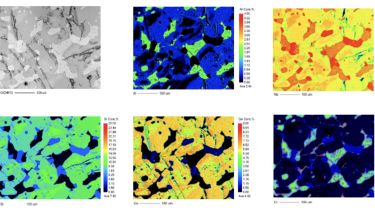
WDS Mapping of Elements in an “As Cast and Heat Treated” NbSi Alloy “EPMA and the expertise provided valuable insight into elemental segregation with an overall aim is to produce an alloy that has enhanced high temperature performance and oxidation resistance.”
Joe Weeks, PhD Researcher under the supervision of Dr. Claire Utton
- Functional Materials and Devices (FMD) - James Killeen (Supervisor: Prof. Derek Sinclair)
-
“The electrical properties of functional oxides depend on close control of the structure-composition relationships. This often requires low levels of dopants (commonly 1 -5 wt.%) to induce a particular type of defect or defect distribution to achieve the optimum performance. Previous attempts at investigating the elemental distribution across grains/grain boundaries of electro ceramic materials in our group (e.g., high permittivity dielectrics for Multi-Layer Ceramic Capacitors or solid electrolytes for Solid Oxide Fuel Cells) via Energy Dispersive Spectroscopy (EDS) has had limited success due to the low level of dopants. The use of EPMA has facilitated: (i) acquisition of high-resolution qualitative maps on the dopant ions (in addition to the main elements present); and (ii) quantitative point analysis data. This has allowed clear determination of how low-level dopants are distributed in the ceramics and the roles they play in controlling the functionality. Additionally, the more quantitative analysis by EPMA has permitted clear identification of minority phases that are challenging to isolate via XRD and EDS. This information has been used to further modify the processing methods in attempts to achieve optimum behaviour. “
“EPMA has been very successful with quantifying low level dopant elements and their distribution within the ceramic capacitors. This information has led to further modifications to the capacitors processing methods to achieve optimum performance.”
