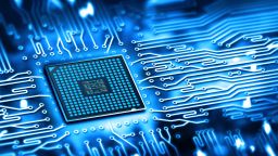
Semiconductor and Quantum Technologies
Our research spans compound semiconductor materials and devices, electronic and optical systems, and chip design for integrated circuits. We host the UK’s largest academic semiconductor epitaxy facilities and an Innovation Knowledge Centre for heterogeneous integration.

Semiconductor Materials & Devices
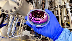
We have been carrying out world leading semiconductor materials and devices research since the 1970s, developing novel compound semiconductors and producing breakthroughs in photonics, electronics and quantum applications. As host of the EPSRC National Epitaxy Facility since 1978, we have been contributing to the vibrant compound semiconductor research in the UK.
Complementing NEF, we have academics who are world leaders in semiconductor epitaxial growth and device design. Current examples include:
- Avalanche photodiodes (APDs) and single photon avalanche diodes (SPADs)
- Single photon emitter based on quantum dots (quantum technologies)
- Novel techniques in epitaxial growths; Epitaxy of novel compound materials
To support our wide-ranging semiconductor research, we maintain extensive experimental facilities for epitaxial wafer growth (Molecular Beam Epitaxy, MBE; Metal-Organic Vapour Phase Epitaxy, MOVPE or MOCVD), device fabrication and wafer/device characterisation.
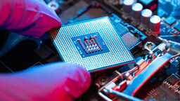
Circuits and Systems
Our academics are experts in microelectronics and instrumentation relying on semiconductor sensors.
We host the UKRI Innovation and Knowledge Centre for Heterogeneous Integrated MicroElectronic and Semiconductor Systems (CHIMES). Working with our academic and industrial partners, we bring together disparate parts of the research and development activity in semiconductor and electronic systems design from across the UK, to provide for Heterogeneous Integration systems the following:
- Reusable design assets
- Manufacturing pathways
- Skill training
We are a key partner in the Semiconductor: Skills, Talent and Education Programme (STEP), a UK government initiative. We work closely with the UK Electronics Skills Foundation (UKESF) to deliver semiconductor skills development courses on chip design flow process and EDA tools used for implementing designs to undergraduates and recent graduate students.
Utilising expert knowledge of semiconductor sensors, our academics carry out research on instrumentation and optical imaging. We have applied these to temperature measurement and imaging for manufacturing, additive manufacturing, and medical imaging of native and engineered biological tissues.
Commercialisation
We have been commercialising our discoveries through spin-out companies. Examples include
- Infinite Design (chip designs; now part of ARM)
- Phasefocus (imaging instruments; now part of Bruker)
- Phlux Technology (infrared avalanche photodiode)
- AegiQ (single photon light source)
- PyrOptik (quantitative temperature measurement)
- Pixel~Flo (microLED manufacturing).
Our research findings have also been utilised in clinical trials, e.g., Skin bioMARkers for atopic eczema Therapy evaluation.
Core members
Materials and Devices:
- Professor John David
- Dr Kristian Groom
- Professor Jon Heffernan
- Professor Mark Hopkinson
- Professor Andrew Maiden
- Professor Jo Shien Ng
- Dr Joe Smith
- Dr Paloma L dos Santos
- Dr Robert Richards
- Professor Chee Hing Tan (Head of Group)
- Dr Thomas Walther
Circuits and Systems: